
Der Charme der Gartengestaltung: Ein Blick auf die Welt des Horts mit Jan Maucher Gartenbau
Llimousine Service

Luxurious and Reliable Transportation with Aston Limo Service
For those seeking
In the rapidly evolving landsc In AI Shorts Generator
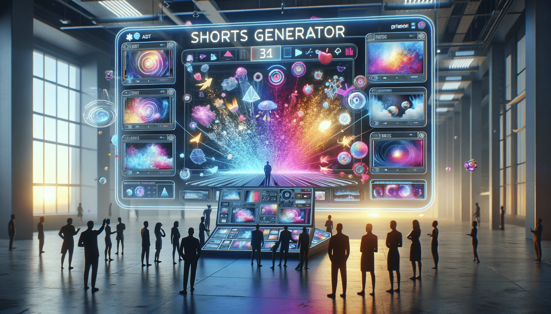
Revolutionizing Content Creation with Faceless AI Video Templates
Joker369

Discover the Thrills of Joker369: A Comprehensive Look
Outranking io
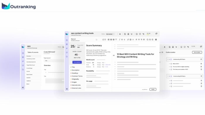
How Outranking.io Revolutionizes Content Creation with AI-Powered SEO Tools